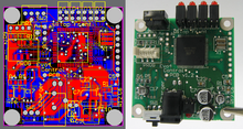
1. Let's talk about PCB--- PCB's History
1. Let's talk about PCB--- PCB's History
Juvtmall ( a company supply PCB Prototyping, PCBA service and sell kinds of components, modules and so on)
The other Blog
Juvtmall ( a company supply PCB Prototyping, PCBA service and sell kinds of components, modules and so on)
Development of the methods used in modern printed circuit boards started early in the 20th century. In 1903, a German inventor, Albert Hanson, described flat foil conductors laminated to an insulating board, in multiple layers. Thomas Edison experimented with chemical methods of plating conductors onto linen paper in 1904. Arthur Berry in 1913 patented a print-and-etch method in the UK, and in the United States Max Schoop obtained a patent to flame-spray metal onto a board through a patterned mask. Charles Ducas in 1927 patented a method of electroplating circuit patterns.
The Austrian engineer Paul Eisler invented the printed circuit as part of a radio set while working in the UK around 1936. In 1941 a multi-layer printed circuit was used in German magnetic influence naval mines. Around 1943 the USA began to use the technology on a large scale to make proximity fuses for use in World War II. After the war, in 1948, the USA released the invention for commercial use. Printed circuits did not become commonplace in consumer electronics until the mid-1950s, after the Auto-Sembly process was developed by the United States Army. At around the same time in the UK work along similar lines was carried out by Geoffrey Dummer, then at the RRDE.
Before printed circuits (and for a while after their invention), point-to-point construction was used. For prototypes, or small production runs, wire wrap or turret board can be more efficient. Predating the printed circuit invention, and similar in spirit, was John Sargrove's 1936–1947 Electronic Circuit Making Equipment (ECME) which sprayed metal onto a Bakelite plastic board. The ECME could produce three radio boards per minute.
During World War II, the development of the anti-aircraft proximity fuse required an electronic circuit that could withstand being fired from a gun, and could be produced in quantity. The Centralab Division of Globe Union submitted a proposal which met the requirements: a ceramic plate would be screenprinted with metallic paint for conductors and carbon material for resistors, with ceramic disc capacitors and subminiature vacuum tubes soldered in place. The technique proved viable, and the resulting patent on the process, which was classified by the U.S. Army, was assigned to Globe Union. It was not until 1984 that the Institute of Electrical and Electronics Engineers (IEEE) awarded Mr. Harry W. Rubinstein, the former head of Globe Union's Centralab Division, its coveted Cledo Brunetti Award for early key contributions to the development of printed components and conductors on a common insulating substrate. As well, Mr. Rubinstein was honored in 1984 by his alma mater, the University of Wisconsin-Madison, for his innovations in the technology of printed electronic circuits and the fabrication of capacitors.
Originally, every electronic component had wire leads, and the PCB had holes drilled for each wire of each component. The components' leads were then passed through the holes and soldered to the PCB trace. This method of assembly is called through-hole construction. In 1949, Moe Abramson and Stanislaus F. Danko of the United States Army Signal Corps developed the Auto-Sembly process in which component leads were inserted into a copper foil interconnection pattern and dip soldered. The patent they obtained in 1956 was assigned to the U.S. Army. With the development of board lamination and etching techniques, this concept evolved into the standard printed circuit board fabrication process in use today. Soldering could be done automatically by passing the board over a ripple, or wave, of molten solder in a wave-soldering machine. However, the wires and holes are wasteful since drilling holes is expensive and the protruding wires are merely cut off.
From the 1980s small surface mount parts have been used increasingly instead of through-hole components; this has led to smaller boards for a given functionality and lower production costs, but with some additional difficulty in servicing faulty boards.
Historically, many PCB measurements were in multiples of a thousandth of an inch, also called "mils". For example, the Dual In-line Package (DIP) and most other through-hole components have pins located on a grid spacing of 100 mils (0.1 inch). Surface-mount SOIC components have a pin pitch of 50 mils. SOP components have a pin pitch of 25 mils. Level B technology recommends a minimum trace width of 8 mils, which allows "double-track" – two traces between DIP pins.The other Blog


评论
发表评论